
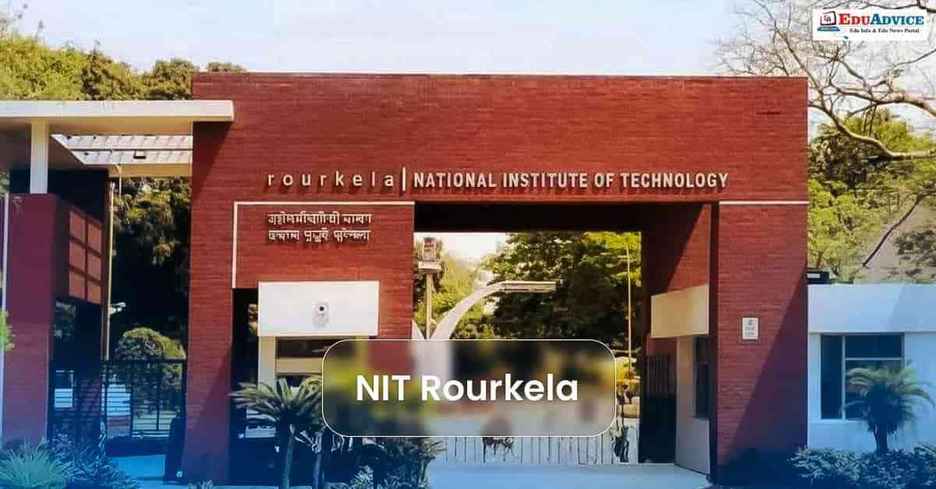
NIT Rourkela’s indigenous design displayed at SEMICON India 2026
Odisha: A semiconductor design conceived at the National Institute of Technology Rourkela (NIT Rourkela) and fabricated in Chandigarh finds a place in the emblem representing the contributions of 20 academic-industry organisations in the semiconductor ecosystem at SEMICON India 2026. The event, held at Yashobhoomi, New Delhi, from September 17-19, also witnessed NIT Rourkela students’ interaction with Prime Minister Narendra Modi.
The chip, ASCON AEAD Security Chip C2S0091, is on display at SEMICON India 2026 as a design from NIT Rourkela. The design was created by the Institute’s PhD student Pradeep Kumar Mohanty under the guidance of Prof. Ayas Kanta Swain and Prof. Kamalakanta Mahapatra, Dept. of Electronics and Communication Engineering, NIT Rourkela.
ASCON AEAD Security Chip (C2S0091) – A lightweight crypto security IC
The chip is part of the academic-industry contributions to SEMICON India 2026. Mohanty belonged to the group of young designers who met PM Modi on the occasion. A brief description of the chip follows: “Our design targets low-complexity, lightweight cryptography security implementations for embedded-IoT applications. These applications require encryption and authentication of data, typically with constrained computing, memory, and energy resources compared to conventional computers. A crypto-processor, therefore, is a promising solution for embedded-IoT systems to implement security functions with lower overheads.
The design of the ASCON AEAD Security IC C2S0091 implements such a crypto-processor in hardware for embedded-IoT applications to accelerate encryption-decryption functions with reduced power, area, and latency overheads.”
Semiconductor design to silicon: Bridging the gap
The significance of the NIT Rourkela achievement lies both in the contents of the design and its successful fabrication in Chandigarh. The design was created under the MoE’s Chip-to-Startup (C2S) Programme of the Ministry of Electronics and Information Technology (MeitY), New Delhi, and fabricated at the Semiconductor Complex Limited (SCL), Mohali.
The design-to-fabrication flow is critical in India’s current semiconductor design and manufacturing push. While it is relatively straightforward for a budding semiconductor start-up to get a design fabricated in a foundry abroad, the entire value chain – from design to verification to fabrication to packaging – is being built or re-engineered within India. The design of the ASCON IC by NIT Rourkela researchers is, indeed, a step forward in this endeavor. However, it is useful to put the achievement in perspective. NIT Rourkela has had programs in semiconductor design for some time. The Institute’s record shows that starting from 1999 under the guidance of Prof. Kamalakanta Mahapatra, the VLSI and Embedded Systems Group at NIT Rourkela has been contributing to semiconductor design, education, and research.
As a C2S design, ASCON IC joins a list of other ICs designed by various academic organisations under the C2S Program. NIT Rourkela’s VLSI Group has had several ICs designed and fabricated in the past, and it showcased its contributions at SEMICON India 2025.
Odisha’s semiconductor initiatives on display
The visit of the Odisha Chief Minister, Mohan Charan Majhi, to SEMICON India 2026 to know about the efforts of NIT Rourkela in developing indigenous semiconductor designs bears testimony to the state’s interest in building a semiconductor ecosystem in the state. The state government is already engaging with potential investors from South Korea, Japan, Europe, etc.
NIT Rourkela, too, is part of the push that is being made in the state for promoting semiconductors. Its contribution to the ecosystem builds upon the existing strengths in electronics design and education, particularly VLSI design, that the Institute has been nurturing since 1999. While the CM’s visits and meetings with investors will help in creating an enabling policy environment, the role of universities like NIT Rourkela will be critical in building India’s semiconductor design ecosystem.
Why NIT Rourkela’s design is important
India’s semiconductor needs are being met by a combination of investments in fabrication plants, foundries, and design companies. Efforts are also being made to enhance the design ecosystem through funding, education, and R&D initiatives. However, what happens beyond design – packaging, testing, and fabrication – is also important.
NIT Rourkela’s involvement in the design and fabrication of the ASCON AEAD Security IC under the C2S Program exemplifies the kind of initiatives that will enhance India’s semiconductor design ecosystem. The participation of academia in such programs is essential to build a talent pool and foster an innovation environment. There is, however, a need to move from individual ICs designed on a prototype basis to actual commercial design realisation with design reuse. NIT Rourkela’s contribution at SEMICON India 2026 will hopefully lead to more such initiatives showcasing India’s semiconductor design capabilities.
Click Here for More Science & Technology